|
Size: 6796
Comment:
|
Size: 7145
Comment:
|
| Deletions are marked like this. | Additions are marked like this. |
| Line 15: | Line 15: |
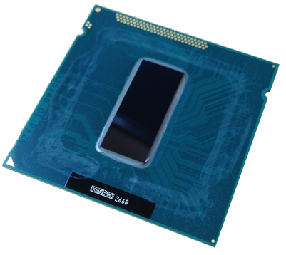
| || {{attachment:ivybridge2.png | | width = 200 }} || This is an Intel Ivy Bridge CPU, with 4 processors and 1.4 billion transistors, attached upside down to a package. The chip is 1.6 square centimeters, and probably thinned down from 750 μm to improve thermal conductivity. If this die was thinned to 200 μm, the silicon would weigh perhaps 85 milligrams. If it was thinned to 20 μm, 8.5 milligrams, about 2 milligrams per processor. A large Google data center might contain a million processors; about 2 kilograms of active CPU silicon - embedded in tons of substrate and packaging, and thousands of tons of circuit boards, racks, wiring and cooling water plumbing. || | || {{attachment:ivybridge2.png | | width = 200 }} || This is an Intel Ivy Bridge CPU, with 4 processors and 1.4 billion transistors, attached upside down to a package. The chip is 1.6 square centimeters, and probably thinned down from 750 μm to improve thermal conductivity. If this die was thinned to 200 μm, the silicon would weigh perhaps 85 milligrams. If it was thinned to 20 μm, 8.5 milligrams, about 2 milligrams per processor. A large Google data center might contain a million processors; about 2 kilograms of active CPU silicon - embedded in tons of substrate and packaging, and thousands of tons of circuit boards, racks, wiring and cooling water plumbing.<<BR>><<BR>>Server sky processors will be rather different than the Ivy Bridge CPU core - running at lower speed and optimized for power efficiency, they will more resemble Intel's processors for handheld devices, without the graphics processing and producing and receiving differential intermediate frequency I and Q signals to external radio chips || |
Integrated Circuit Mass
How Much does a Chip Weigh?
CMOS (Complimentary Metal Oxide Semiconductor) integrated circuit chips are made N type and P type MOS field effect transistors, wiring, insulators, on top of a silicon substrate. The zoo of devices on all varieties of integrated circuits includes bipolar transistors, diodes, capacitors, loop inductors, diffused and thin-film resistors, sometimes even special sensors like avalanche photodiodes. However, almost everything we do with server sky will involve advanced-process CMOS, with some DRAM ( Dynamic Random Access Memory ) using stack capacitors and some flash (block rewritable) EEPROM ( Electrically Eraseable Programmable Read Only Memory, which writes information by trapping charges in the insulators of MOS gates.
|
These are all planar processes produced by photolithography. All structures are made by deposition and etching of materials, and are typically very thin, a few micrometers. High power integrated circuits, such as 150 watt microprocessors and GPUs, are somewhat thicker, because the uppermost layers of interconnect metal are thick and low resistance to handle up to 100 amps of power. The lower signal handling metal layers are thin and optimized for low capacitance wires, perhaps half as thick as they are wide (a fraction of a micrometer). |
Server sky chips will use low power varieties of these advanced processes, with fewer metal layers and no fat upper layers because each chip will be small and use milliamps rather than amps. We can expect the thickness of the active layers of chips to be less than five microns thick.
Integrated circuit chips are built on large wafers, 30 centimeters or more in diameter. The wafers are typically 750 μm (micrometers) thick for mechanical stiffness during manufacturing. After the planar circuitry is completed, the wafers are "backlapped", ground down on the back side to make them thinner. Then they are sawn into individual die ( == chips ). The backlapping is a coarse grinding process, and variation in the process limits the thinness of the resulting die, but 50 μm thick is a typical result, good enough for cell phones and other volume-constrained products. The die can be made much thinner, as low as 20 μm or even 7.5 μm, for attachment to paperthin substrates in applications such as RFID tags. Such paperthin die are more flexible and more resistant to fracture, and the processes for making thin chips reliably will (hopefully) be widespread and very inexpensive when thinsats are produced by the billions.
The density of silicon is 2.65g/cm3, so a 20 μm layer of processed silicon weighs about 5 mg/cm2.
|
This is an Intel Ivy Bridge CPU, with 4 processors and 1.4 billion transistors, attached upside down to a package. The chip is 1.6 square centimeters, and probably thinned down from 750 μm to improve thermal conductivity. If this die was thinned to 200 μm, the silicon would weigh perhaps 85 milligrams. If it was thinned to 20 μm, 8.5 milligrams, about 2 milligrams per processor. A large Google data center might contain a million processors; about 2 kilograms of active CPU silicon - embedded in tons of substrate and packaging, and thousands of tons of circuit boards, racks, wiring and cooling water plumbing. |
|
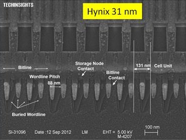
DRAM Hynix 62x93nm (31nm 6F?) DRAM cell. A gigibyte of RAM has an area of 0.6 cm2, including some periphery and error-correction processing. At 20μm thick, that is 3 mg/GiB, or 330TiB/kg |
|
Solid State Flash Memory. Cross section of a 27nm Samsung NAND flash array. Intel and Micron offer a 25 nm, 64 gigibit, 1.31 cm2 3 level flash memory. Thinned to 20nm, that is 0.8 mg/GiB, or 1.2PiB/kg |
|
Memory will have additional logic to do error correction after access and before refresh. It will likely be optimized to run at higher power efficiency and lower speed than terrestrial applications like desktop CPUs |
|
Google Data Center - est. 100 lb/ft2 including structure, 200,000 sq ft, 1 million kilograms. |
A 256 core, 512 GiB flash, 16 GiB dram processor array at $10/g launch cost, active silicon only, NOT including substrate, solar cell, wiring, etc:
component |
density |
weight |
component cost |
launch cost |
256 processors |
2mg/proc |
512 mg |
?? |
$5.12 |
512 GiB flash |
0.8mg/GiB |
410 mg |
|
$4.10 |
16 GiB dram |
3mg/GiB |
48 mg |
|
$0.48 |
Total |
|
970 mg |
|
$9.70 |
If this represents the capability of one thinsat, and an array of 8000 thinsats weighs 40kg, then multiply the above compute power by 8000 for a launch cost of $400K, including power supply and radio ground link. Arrays share flash storage, so the flash memory capacity of the entire array would be 4 petabytes.


